State‑of‑the‑art atomistic quantum transport for next‑generation nanoelectronic devices
The atomistic eXplorer, atomX, is a high‑performance dissipative DFT‑NEGF simulator with unique capabilities in terms of efficiency, speed and memory footprint. It brings first‑principles accuracy together with affordable simulations including scattering —so you can explore realistic devices with up to millions of atoms and go from materials to I‑V characteristics with confidence.
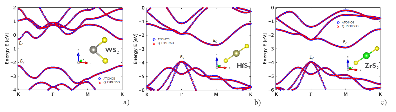
atomX is the fruit of over 20 years of advanced research in quantum transport and device physics. It benefits from the best technologies optimized over the years and validated over a wide range of devices and material systems.
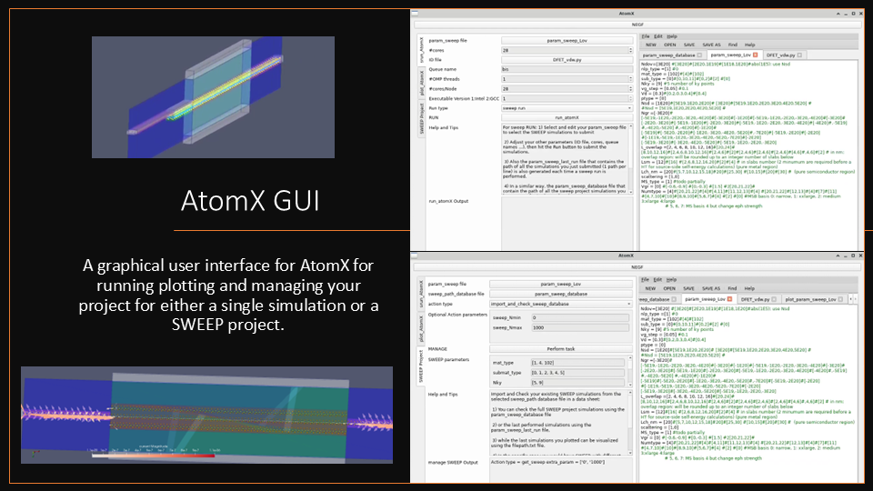
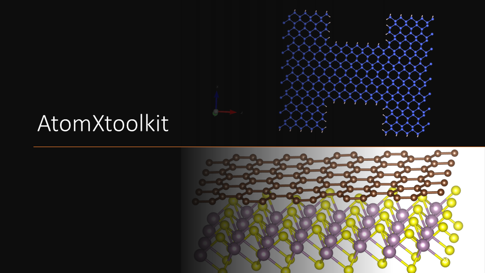
atomX is packaged with its companion Tool Kit (AtomXtoolKit) for easy and automated DFT-supercell building and optimization and AtomX GUI, a powerful integrated graphical user interface for automated parameter studies and post‑processing.

Afzalian, A. Ab initio perspective of ultra-scaled CMOS from 2D-material fundamentals to dynamically doped transistors. npj 2D Mater Appl 5, 5 (2021)
Why traditional approaches fall short
Gaps in today’s exploration workflows
- Emerging materials and interfaces demand atomistic, parameter‑free models to avoid guesswork and capture full‑band effects.
- Engineering‑relevant simulations require realistic device sizes and dissipative physics—not just idealized ballistic models.
- Teams need repeatable, automated flows from supercells to device results for rapid learning cycles.
What this means in practice
- Slow, memory‑heavy runs limit design‑space exploration.
- Interfaces/contacts and heterostructures are hard to capture with simplified models.
- Manual supercell creation and data wrangling adds friction and inconsistency.
atomX: from atoms to device‑level insight
atomX combines ab‑initio DFT‑based Hamiltonians with a dissipative, self‑consistent NEGF solver to predict transport with high fidelity—covering quantum confinement, tunneling, and scattering by construction.
Use DFT‑NEGF for novel materials and interfaces, or switch to tight‑binding / effective mass where speed matters. Evaluate materials, contacts, stacks, and device geometries—then deliver clean I–V and band/DoS analyses.
Key features & benefits
Ab‑initio accuracy
DFT‑based Hamiltonians (plane‑wave + Wannier or localized orbital) feed directly into NEGF—parameter‑free for new materials.
Interfaces & stacks
Model explicit contacts and van der Waals heterostructures to optimize SBH and tunneling.
Speed & scale
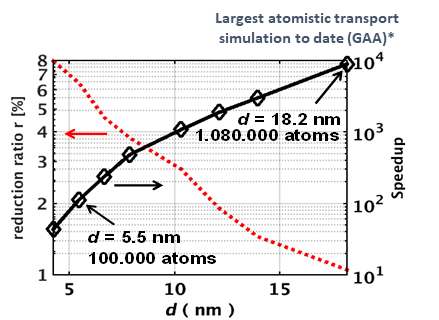
Massively parallel solvers, memory‑lean data structures, and mode‑space acceleration for practical runtimes with large devices up to millions of atoms.
Scattering included
Accurate electron–phonon scattering with self‑consistent Born approximation; DFPT‑derived options available.
Automation & sweeps
AtomX GUI: a powerful integrated graphical user interface (also Python interface with SWEEP library) for automated parameter studies and post‑processing.
AtomXtoolkit
Automate supercell creation/relaxation/merging and integrate with common DFT packages.
Technology that enables results
- High‑performance core: hybrid MPI/OpenMP C++ solvers with sparse, memory‑lean data structures.
- Self‑consistent convergence: predictor–corrector Poisson‑NEGF methods and smart adaptive damping for robust solutions.
- Acceleration: mode‑space NEGF workflows delivering typical 100× speedups on suitable supercells.
- Scattering physics: state-of-the-art self‑consistent Born formalism, with options from isotropic deformation potentials to DFPT‑derived full matrices.
- Load balancing: recursive adaptive energy‑grid with master–slave scheduling to catch resonances efficiently.
Where teams use atomX
2D material transistor screening
Quantify material choice, layer‑count, orientation, and channel‑length trade‑offs; assess mobility and current to shortlist candidates.

2D materials screening (ION vs L, mobility, DoS).
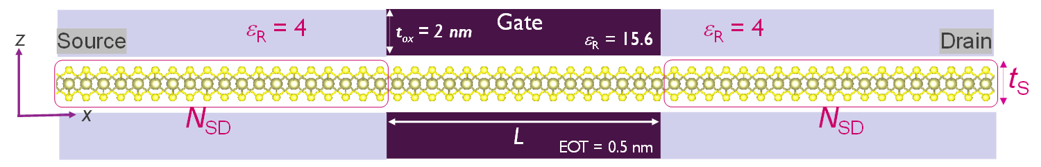
Explicit contacts & interfaces
DFT-NEGF transport across metal /semiconductor interfaces enabling efficient material screening and contact engineering.
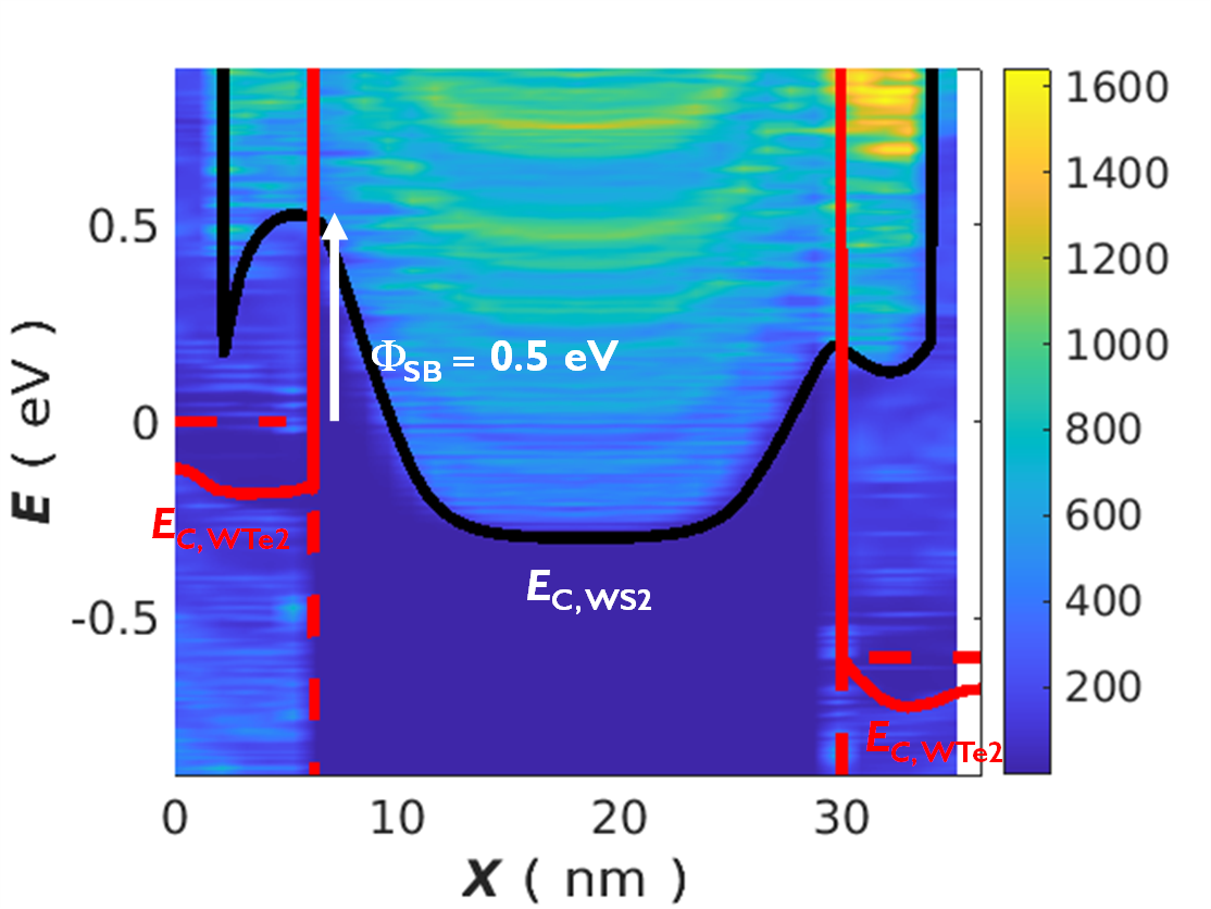
Interface transport.
Novel device concepts
Explore Dirac/"cold source" FETs, van der Waals TFETs, or devices based on topological materials; study fundamental physics, sensitivity to scattering and materials.


Cold source Dirac FET study.
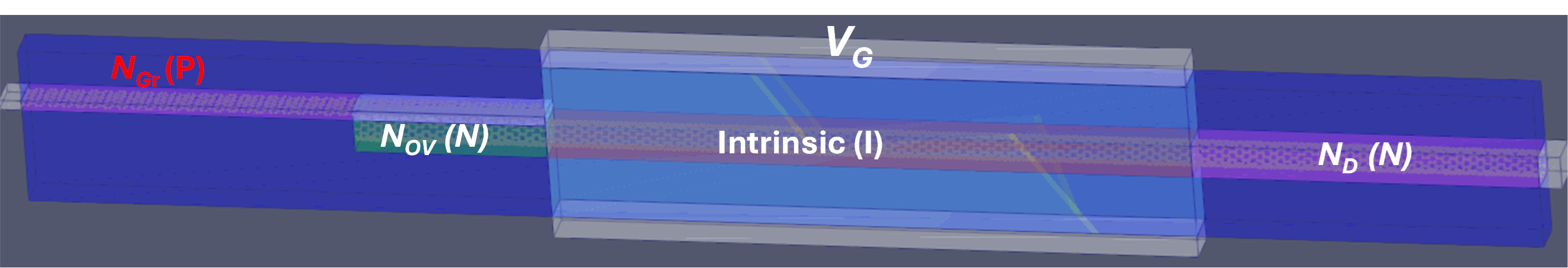
CNT‑FET fundamentals
Hybrid‑functional DFT for accurate bandgaps analyze BTBT limits (IMIN) and ION vs. VDD.

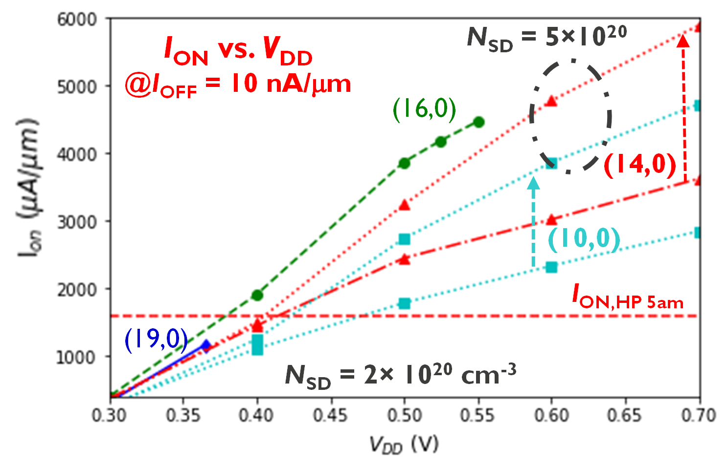
CNT‑FET fundamentals.
BioFET simulations
Include ions in solution and electrode models to study single‑molecule detection (e.g., DNA sensing).
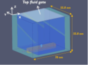

BioFET sensing behavior.
Limit of scaling of Si Nanosheets
Surface‑roughness‑driven variability and short‑channel effects for ultrascaled Si/Group‑IV.
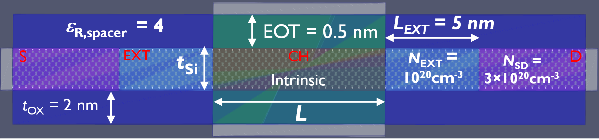
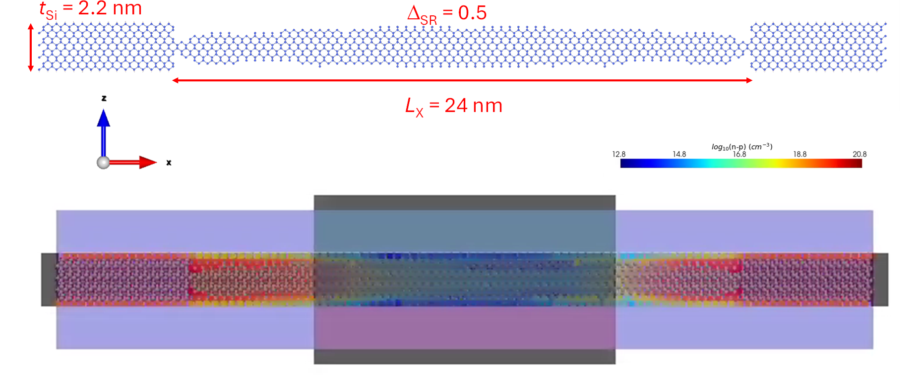
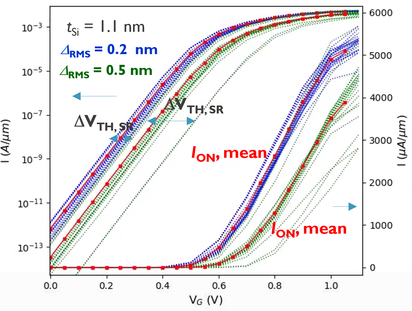
Surface roughness & variability.
Performance & validation
- Agreement with experiments: the deck highlights close match between simulations and WSe₂ device measurements.
- Scale & efficiency: designed for realistic devices; publications show million‑atom capability and efficient ab‑initio transport at scale.
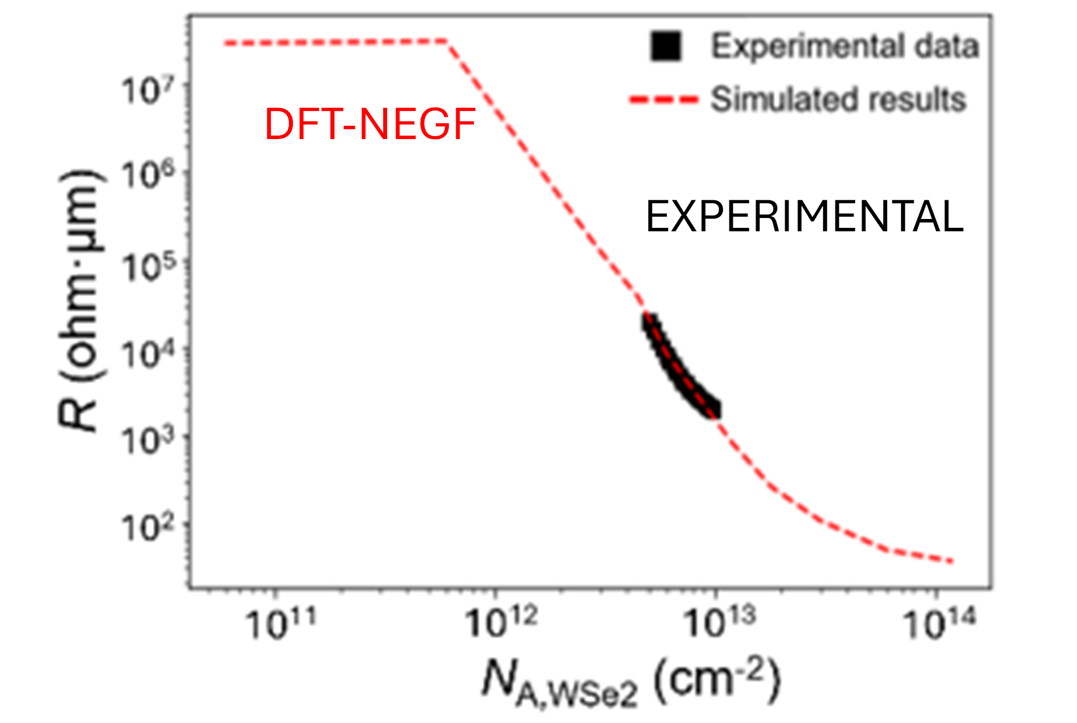
Experiment ↔ Simulation agreement (WSe₂ contacts).
Fits your workflow
- DFT sources: plane‑wave (e.g., QE, VASP) with Wannierization, or localized orbital DFT (e.g., OPENMX, CP2K) without Wannierization.
- Automation: AtomXtoolkit to build and relax supercells; AtomX GUI A graphical user interface for running, plotting and managing your SWEEP projects.
- From atoms to I–V: assemble material building blocks into full device geometries and run transport for clean results and plots.
See atomX in action
Ready to evaluate atomX for your materials and devices? Request a live walkthrough, discuss your use case, or ask about licensing.
Prefer to share slides or device targets first? We’ll suggest a minimal validation plan and next steps.
What to expect
- 30–45 min discovery + demo tailored to your workflows.
- Guidance on models (DFT‑NEGF vs TB/effective mass) and runtime/scale expectations.
- Optional follow‑up with trial access or a pilot study proposal.